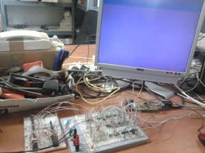
In the picture below you can see a minimal prototype of a Z80 based computer connected to a prototype of VGA display. There is only CPU, ROM and I/O decoder (no RAM). The setup works OK!
The code burned in a FLASH ROM chip looks like this: (filling the screen with sequential colors):
ld d,0
ld bc,64000
rysuj:
ld a,b
out (1),a
ld a,c
out (2),a
sprawdzaj:
in a,(5)
bit 0,a
jr z,sprawdzaj
sprawdzaj2:
in a,(5)
bit 0,a
jr nz,sprawdzaj2
ld a,d
out (3),a
dec bc
sub a
cp c
jr nz,rysuj
sub a
cp b
jr nz,rysuj
ld bc,64000
inc d
jp rysuj
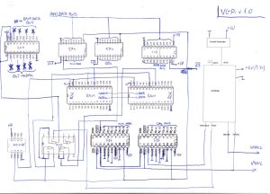
Below you can see a sketch of a VGA display circuit – it explains the basics of this simple VGA display adapter operation. The final version is a little bit different from the picture below: there are now 3x buffers instead of 2xlatch + 1x buffer on the input side, and also Attiny13 has beed replaced with 7474 chip as described in the text later.
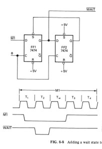
Attiny13 in the write delay section has been replaced with 7474 flipflops in a configuration shown below:
This circuit works OK at full 4Mhz speed (Attiny version worked only with 1Mhz clock)
On the picture, /M1 signal is a chip select signal from the address decoder in my circuit (and opens all buffers on the VGA adapter – switching to write mode). /WAIT signal is a /WR signal for RAM. Fi clock signal is 4Mhz from CPU. This 7474 configuration allows a proper /WR delay for writing to RAM chips.
Second issue:
Despite of several tries, I couldn`t properly synchronize writes to RAM with VGA sync signals in hardware, which results in an effect of black stripes and dots on the display during Video RAM writes. The problem was partialy resolved in software with a little modification in the circuit. An additional 74LS244 buffer was introduced. The buffer was activated by I/O decoder (only /IORQ + /RD in the prototype). The CPU can pool for VOUT signal from the VGA adapter trough that buffer and wait for the falling edge of it. After detecting the falling edge, the CPU may start the write cycle. This way, the CPU writes only during the horizontal/vaertical blanking time, which eliminates the snowing effect. The drawback of this solution is of course a decreased troughput. On the other hand, a possibility of software control over Video RAM write mechanism choice is fully available: We can use VOUT information to eliminate snow, or we could ignore it, allowing faster transfers (for example in a clear screen operation). There is also a possibility to keep track of more VGA timming signals trough the 74LS244 buffer (HSYNC/VSYNC/VENABLE) and use them for optimisation of Video RAM access.


