Mass storage solution for my C-Z80 computer is now ready. I`ve been doing some research on the CF card lately, and I`ve come to the conclusion that interfacing the CF card in 8-bit true-IDE mode is really easy. In fact, the whole IDE interface proved to be a simple and straightforward way of connecting CF cards and hard drives to 8-bit microprocessor or microcontroller. However, I`ve choosen the CF-card instead of a regular IDE harddrive, mainly because of the 8-bit mode that can be used with CF-Card in true-IDE mode. Hard disks are using 8-bit data bus for commands, but a 16-bit one for the actual data. There is no problem in using a standard IDE hard disk with 8-bit only interface, but: we are losing half of the drive`s capactity, and what`s more important: we cannot use any standard filesystem in this way.
I`ve been taking some tips in my design from these sites:
Grant Searle`s CP/M machine:
http://searle.hostei.com/grant/cpm/index.html#Schematic
Grant says he used CF cards connected directly to Z80 bus without any problems. I wasn`t so lucky though: While breadboarding I`ve discovered that only one card worked correctly when connected directly (SanDisk 2GB). Others that I`ve tested didn`t worked (Cisco 64MB: every 3-4th byte read was corrupted, Kingston 4GB – freezed the system, probably was permanently selected). After adding 2x74HCT245 buffers everything worked perfectly – all cards gave good readings, even using very long IDE cables.
Daniel Tufvesson`s blog:
http://www.waveguide.se/?article=8-bit-compact-flash-interface
Very nice quick overview of the 8-bit true-IDE mode of the CF card and an excellent source code example – helped me a lot and pushed the work forward.
Peter Faasse`s document on IDE interface for a microcontroller:
https://www.pjrc.com/tech/8051/ide/wesley.html
Absolutely brilliant text on the subject. Clear and simple. Reading it was a pure pleasure. Practical description of IDE registers and commands.
Lo-tech ISA CompactFlash Adapter rev. 2
http://www.lo-tech.co.uk/wiki/Lo-tech_ISA_CompactFlash_Adapter_revision_2
I recommend this design very much. I`ve build my own piece using the schematics provided on the page – it is working perfectly in my PC-XT machine.
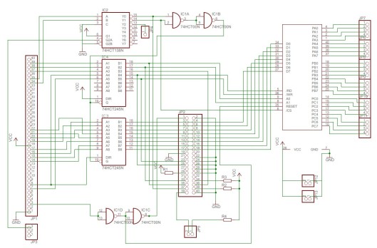
My implementation of the 8-bit IDE interface for C-Z80 computer uses the FFC0h base address. I`ve also added a 8255 Parallel I/O as a bonus. This chip is placed at the FFD0h base address.
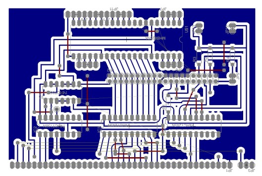
Schematics and PCB: I didn`t bother with elegant design at all – some connections are made with cables. D8-D15 pins of the IDE connector have been removed to simplify the design even more.
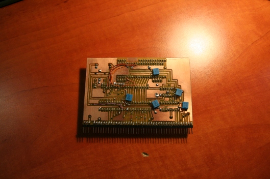
The assembled card looks like this:
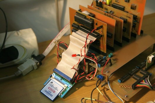
Connected to the system:
Now some tests. I`ve written a small test program which reads one sector of a CF card and stores it in RAM, so it can be examined with ROM Monitor`s “dump” command. The sector addressing uses LBA mode. As an example,the program will read the MBR of a CF card. Here is the code:
DELAY: .equ 04ceh
DELAY_NORMAL: .equ 04eah
DELAY_LONG: .equ 04dch
x_kursora: .equ 85a8h
y_kursora: .equ 85A9h
write_message: .equ 0619h
erase_screen: .equ 04f8h
.org 0a000h
start:
call erase_screen
call cf_rdy_wait
call cf_init
call cf_info
ld a,0h
ld (lba0),a
ld a,0h
ld (lba1),a
ld a,0h
ld (lba2),a
ld (lba3),a
call cf_read_sector
; ld ix,buffer
; call cf_sector_descramble
loop2: jp 0000
cf_read_sector:
call cf_wait
call cf_set_lba
ld bc,0ffc2h
ld a,1 ; czytamy 1 sektor
out (c),a
call cf_wait
ld bc,0ffc7h
ld a,20h
out (c),a ; sector read command (20h) to command register (base+7)
call cf_error_check
ld ix,buffer
call cf_read
ret
cf_set_lba
ld a,(lba0)
ld bc,0ffc3h
out (c),a
ld a,(lba1)
ld bc,0ffc4h
out (c),a
ld a,(lba2)
ld bc,0ffc5h
out (c),a
ld a,(lba3)
ld bc,0ffc6h
and 0fh ; mask 4 MSBs of LBA3 byte
or 0e0h ; sets LBA mode + MASTER drive
out (c),a
ret
cf_rdy_wait
ld bc,0ffc7h
in a,(c)
and 40h
jp z, cf_rdy_wait
ret
cf_wait:
ld bc,0ffc7h
in a,(c)
and 80h
jp nz,cf_wait
ret
cf_init:
ld bc,0ffc7h
ld a,04h
out (c),a
call cf_wait
ld bc,0ffc6h
ld a,0e0h
out (c),a
ld bc,0ffc1h
ld a,01h
out (c),a
ld bc,0ffc7h
ld a,0efh
out (c),a
call cf_wait
call cf_error_check
ret
cf_error_check:
ld bc,0ffc7h
in a,(c)
and 01h
jp z,no_error
ld ix,error_msg
call write_message
loop:
jp loop
no_error:
ret
cf_read:
call cf_wait
ld bc,0ffc7h
in a,(c)
and 08h
jp z,no_more_data
ld bc,0ffc0h
in a,(c)
ld (ix),a
inc ix
jp cf_read
no_more_data:
ret
cf_info:
call cf_wait
ld bc,0ffc7h
ld a,0ech
out (c),a
ld ix,buffer
call cf_read
ret
cf_sector_descramble:
ld b,0ffh
cf_descramble_continue:
ld a,(ix+1)
ld d,(ix)
ld (ix),a
ld (ix+1),d
inc ix
inc ix
djnz cf_descramble_continue
ret
error_msg:
.db 10,”CF Error.”,10,0
lba0:
.db 0
lba1:
.db 0
lba2:
.db 0
lba3:
.db 0
.db “**********************************”
buffer: .FILL 1024,0
.END
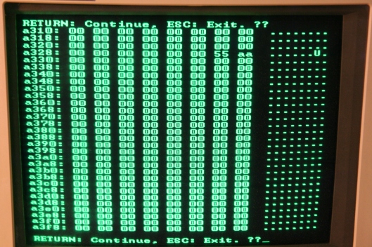
And here we can see the results from the “dump” command. The whole 512byte MBR sector of a CF Card.
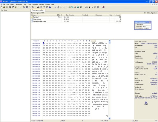
We can compare the results with a dump from Winhex, according to this program, the first sector looks like this:
It seems the CF-Card interface is working fine.
The 8255 chip was tested only in a basic way. I`ve initialized it with “output ffd3 80” command to set all ports to output, and observed the voltage on port B pins when executing “output ffd1 ff” and “output ffd1 00” commands. The chip worked as expected: voltage changed from 0V to ~5V.
Plans for the future:
Implementing FAT16 – It`s quite a challenge when programed in Z80 assembly, but there are lots of very good resources on the web, and I believe it could be done.
Bank switching – A small step towards CP/M in the future. I`ll add a small add-on board on the mainboard, that will allow me to disconnect the ROM memory and place 32K ram chip in it`s place. This way there will be 64K RAM available to the system after booting (ROM code will be copied into the RAM during boot)
Case design – I`m going to ask a skilled craftsman for help in design of a wooden case for the computer.

