
Inspired by the MOS KIM-1 and 8051 based AVT2250 computer that I used to own many years ago,I`ve decided to build my own single board computer that would allow me to learn 6502 assembly and test 65xx family ICs. My goal was to build a single board computer that would be simple, flexible and as useful as possible. I believe I`ve achieved this goal with my new 6507 SBC computer:

The reason I`ve choosen 6507 instead of 6502 is trivial: I had one piece laying around in my ICs box. This particular chip was salvaged from a dead Atari 2600 board and I wanted to put it to a good use. 6507 is basically the same CPU as 6502 but it lacks A13-A15 address lines (which limits it`s address space to 8K) an unfortunatelly also /INT and /NMI – this limits educational value of my SBC a bit as it can`t be used to test/learn interrupt handling. Besides that, all other aspects of 6502 programming and interfacing can be learn with this board.
6507 SBC system consists of the following key components:
- 6507 CPU @ 0.9216 Mhz
- 4KB RAM
- 2KB ROM
- 16450 UART @ 38400 bps
- 16×4 LCD display (HD44780)
- 6526A Complex Interface Adapter (CIA) (for keyboard and general purpose 8-bit parallel port)
- Address decoder with one additional chip select for external peripherals
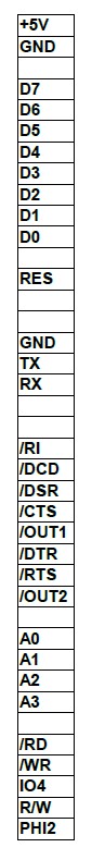
- Expansion connector including: Data bus, A0-A3 address bus, UART signals , CPU signals, reset, power, address decoder signals.
UART RX,TX and GND pins of expansion connector are directly compatible with popular PL2303 USB/UART converter, as shown on the photo above.
Memory map of 6507 SBC system:
- 0000-0fff : user RAM area (4KB, 0200h program entry point)
- f000-f1ff : UART
- f200-f3ff : LCD
- f400-f5ff : CIA
- f600-f7ff : IO4 (additional “chip select” signal for external peripheral)
- f800-ffff : ROM (2KB)
ROM chip contains monitor program with following functionality:
- Downloading data/code from PC using UART.
- Executing code starting from given address.
- HEX dump of memory.
- Editing contents of memory.
There is still several hundred bytes of ROM space available for additional feature.
Expansion connector pinout, from top to bottom:
Here is a small example program. It writes Y register contents to CIA PORTB, waits for some time (using delay fuction from ROM memory), then increases Y register and starts over again. If we connect LEDs with resistors directly to PORTB of CIA, we could see pretty binary counter in action:
0001   0000               CIA_PORTB		.EQU 0f401h
0002   0000               CIA_DDRB		.EQU 0f403h
0003   0000               DELAY			.EQU 0fc24h ;routine from ROM
0004   0000
0005   0200                   .org 0200h
0006   0200
0007   0200              start:
0008   0200 A9 FF               lda #0ffh
0009   0202 8D 03 F4        	sta CIA_DDRB
0010   0205 A0 00       	ldy #00
0011   0207            	 mainloop:
0012   0207 8C 01 F4        	sty CIA_PORTB
0013   020A A9 80       	lda #80h
0014   020C 20 24 FC    	jsr DELAY
0015   020F C8                 	iny
0016   0210 4C 07 02        	jmp mainloop
0017   0213
0018   0213
0019   0FFF                   .org 0fffh ;memory filled up to 4K
0020   0FFF FF                .db  0ffh	 ;dummy byte at the end of 4K
0021   1000
0022   1000                   .ENDtasm: Number of errors = 0
The program (in binary format) can be uploaded to RAM using UART or can be typed in directly by keyboard!
Below, I`m posting photos of prtotype on a breadboard, schematics and PCB design in eagle:


All project files: schematics, board layout, monitor program source and binary can be downloaded from the “download” section.
You may also check out my Youtube video about this project:

Thank you for sharing your work, Michal. Very nice looking build. Cheerful regards…
LikeLike
Thanks Mike, glad you like it 🙂
LikeLike
I found this article very informative. Thank you.
LikeLike
Beautiful work!! Thanx for sharing it.
LikeLike
I love it!!! Amazing 😊
LikeLike
Very nice design. So good to see a 6502 design again. Love the use of a multiline lcd display as well. Where tho did you get the hex keypad? Love that small keypad entry. So much better than descrete switches. Who makes that and where?
LikeLike
Hi, thanks, glad you like my work 🙂
The keypad is an “unique item” sourced many years ago from some sort of security/alarm device. It spend many years in a scrap box waiting to be reused somewhere and finally found it’s place in this SBC 🙂
LikeLike
I just saw the back of the board which looks “hand made with a pen” Very nice work making that. The 6502/07 is a very cool micro. I have had one in my lab for years…lol..no decades.
LikeLike
Thanks! the bottom side is more of an effect of poor craftsmanship than anything else 😀 Heat transfer method is not my best skill. Recently tried photoresistive and it works way way better ! 650x are cool to program. I really have to take some time to write a simple game like tetris , that would make use of the TMS chip of the multimedia board add-on for this SBC…
LikeLike
Hi, thank you for sharing your design.
Would you confirm the values for r1&r2 as well as the capacitors and electrolytic types.
Could you provide a picture of the underside showing the ceramic disc capacitor in the decoupling locations.
Thank you.
Regards
LikeLike
Hi Frank, sorry for late reply… R1 and R2 values are not critical, they should be around 5K to 10K. In my board there are values of 7.5K and 3.3K respectively. Most people are using 10K for all such kind of pullups. All electolytics are 10uF / 25V. ceramics are 100nF.
Here is the photo of the bottom side:
https://drive.google.com/file/d/1MaOLmTfGo0OxzqTaHC_AIPgn7UglVA1A/view?usp=sharing
There were some small corrections as you see.
If you have any questions – please contact me.
LikeLike
Thank you that, one more question, the monitor program, when burning to the EPROM does it go in at 0000 or at F800 ?
LikeLike
Changed the resistor to 8k2 added the 100n decoupling capacitors and hey presto the board powered on to the menu. Thank you for your assistance.
LikeLike
Hello Frank, Yes, you`ve figured it out before my answer 🙂 ROM binary goes to (E)EPROM at 0000h, but in the system, the address will be properly decoded to the same as in .ORG directive. Good job for building my project ! You must definitely send me pictures of it ! 🙂
LikeLike
Hi – quick question on the 4*16 display, I am just getting the parts together to build the board but am struggling to fine a display that matches the board drillings – I am guessing this is because the Eagle part you have used is for a 16×2 display ?
LikeLike
Hi, yes, I`ve used 16×2 part from Eagle, so drill holes will not fit the actual used 16×4 LCD ones. Good news is that 3 holes will have a clear places on the PCB anyway, so it is perfectly fine to just drill them in appropriate place after the board is ready. I`ve actually skipped the drilling, as the LCD sits very firmly soldered directly with a 1×16 goldpin header. The plastic base of the 16 pin goldpin header gives enough space so even the LCD is nicely spaced from the PCB with the metal frame knobs beneath the LCD PCB. If you need some additional photos or info – I can send you some. Please send me some photos after you finish your build, I would be very happy to see them 🙂
LikeLike
Thanks for the info will do on the picture front. The only other part I cannot easily find is the crystal, if you do another pcb relay it would be good to add pads to take the rectangle shaped versions which seem more common these days
LikeLike