Today I`ve connected a standard 16450 UART (NS16450N from National Semiconductors) to my Z80 computer . The connections and chip operations proved to be really easy. Before I start the breadboarding I was concerned about the chip count I would need to use in order to run this thing: the UART chip uses a logic “1” for active RESET and INT signals, so it means that I have to use 74xx04 hex inverter besides 74xx32 or 74xx138 ICs for address and control signals decoding. However, thanks to additional chip select pins on the 16450 and additional address decoder on the C-Z80 expansion board I was able to use only 74xx04 for address decoding, chip activation and also RESET and INT signals inversion. Here is how it`s done:
C-Z80 System NS16450 UART
A7 ————————————– CS0
A6 ————–|>o——————– CS1
/IOREQ+NAND(A8-A15) ———— /CS2
/RESET ————-|>o ————– MR
/INT —————-o<|—————- INTR
This circuit places the UART in I/O address space ff80h – ff87h (it also uses A0-A2 for it`s internal registers addressing) and takes care of proper RESET and INT signals logic levels (Interrupts are not used in the tests, but I plan to enable them as an option)
For the test purpose I didn`t connected MAX232 circuit for voltage level conversion, but instead I used my handy RS232-to-TTL converter connected to PC`s COM1 port.
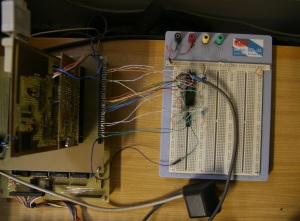
Here is a picture of the whole circuit on a breadboard connected to expansion port on the computer:
Based on the information from the NS16450 datasheet, I`ve issued a set of commands from the ROM Monitor which caused the UART to send three bytes to PC with Teraterm runing. Here are the commands with description:
output ff83 83
; Sending ‘10000011’ to Line Control register: sets the 8bit data 1bit stop , no parity check operation. It also enables the Divisor Latch registers to be accessible.
output ff80 0c
output ff80 00
; Sets the Divisor Latch registers to value 12 (dec). According to datasheet, this value sets the baudrate to 9600 bps when using 1.8432Mhz crystal (which is the one I`m using)
output ff83 03
;Exiting the Divisor Latch mode and returning to normal operation, keeping the previously selected mode of operation.
output ff80 41
output ff80 42
output ff80 43
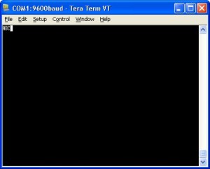
;These commands send the “ABC” string to Transmitter Holding Register, and therefore to the PC. On the PC side we can see the results:
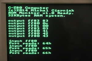
For the receiver test I`ve been pressing the “d”, “e” ,”f” keys on the PC and after each keypress I`ve been doing an input operation from the receiver buffer (ff80h – the same address as the Transmitter Holding Register) on the C-Z80 side. The effect is shown below (there are also previously tested output commands visible on the screen):
Hex “d”, “e”, “f” ASCII characters are read from the Receiver Buffer.
It was extremally easy to test the UART when the ROM Monitor and it`s functions were available – I haven`t even used a single assembler instruction for this: built in input/output commands and keyboard/screen subroutines in ROM were all that I needed. Now the circuit is ready to be taken trough the Eagle Layout Editor to the PCB board and plugged to the C-Z80 expansion board.
For the tests I`ve beed using information from NS16450N datasheet, avalable at:
http://www.datasheetarchive.com/dlmain/Datasheets-8/DSA-150003.pdf
and I`ve also taken some hints from Thomas Scherrer website:


